The Xillybus IP core was implemented on a Virtex-5 FPGA on a Xilinx xupv5lx110t board. The core ports were connected to ChipScope integrated logic analyzer for on-chip testing. Before integrating the Xillybus IP core into the spike-based data reduction platform, its performance was first tested by transmitting predefined data read from a ROM on the FPGA to the host PC. This test was set up to mimic the Xillybus operation in the spike-based data reduction platform. The spike waveform data, to be transmitted to the PC was saved on intermediate buffers then read by the FIFO before transmission using the Xillybus core. The testing data was created using MATLAB® and stored in a .coe file to initialize the ROM having the same size as the spike detection buffer 18×6144. The implementation setting is illustrated in Fig. 1.
On the FPGA side:
The design was implemented on a Xilinx xupv5-lx110t board. The implementation user constraint file was modified accordingly. The transceiver block GTP0 was used on the GTP tile assigned for PCIe transmission GTP_DUAL_X0Y2. The integrated endpoint block differential clock pair PCIE_REFCLK_P and PCIE_REFCLK_N is locked to AF4 and AF3 respectively. The pair is driven by an external PCIe source through the PCIe edge connector, and not driven internally. The clock frequency is 100MHz. The integrated endpoint block reset signal PCIE_PERST_B_LS is available on a CPLD and was locked to W10. The 100 MHz clock provided by the PCI Express connector is connected directly to the Virtex-5 FPGA to clock the PCI Express Endpoint Block Plus LogiCORE. It can be used to clock the internal logic on the FPGA or scaled to match the timing restrictions and latency requirements of the design used.
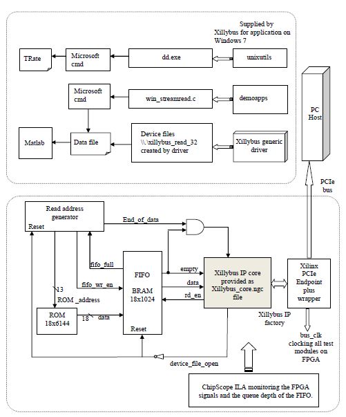
Fig. 1 Xillybus implementation and evaluation setting. The lower box includes the modules on the FPGA end. The upper block includes the software used on the PC host end to retrieve the transmitted data and measure the transmission rate.
On the host side:
For any Xillybus IP core configuration, the streams and their attributes are detected by the Xillybus as it is loaded into the host’s operating system, and device files are created accordingly. In the testing setting designed for transmitting 18-bit words from FPGA to host, the data width option on the Xillybus IP core was 32 bits, and the corresponding port assignments and attributes were used, and the 14 most significant bits were set to 0. Correspondingly the driver creates the device file \\.\xillybus_read_32.
As sample host applications, Xillybus supplies C command line programs that were used in the evaluation setting. The application ‘winstreamread.c’ reads the streaming data from the device file and sends it to standard output. For proper operation, the translation mode was modified to binary mode, to suppress the LF (line feed 0A) character translation to CR-LF (carriage return-line feed combinations 0D 0A), that was observed in the data file.
Unfortunately the Xillybus driver does not offer any time stamping options to be able to track the exact transmission rate. It supplies a ‘dd.exe’ application file which copies data blocks from the device file and then indicates the corresponding transmission rate. For identifying the transmission overhead, sequential data was continuously read from the ROM at the same clock rate (bus_clk), used by the Xillybus IPcore and supplied by the PCIe Endpoint Plus Wrapper LogiCore of 100MHz. The internal signals were monitored using ChipScope and screenshots are shown in Fig 2a and Fig 2b to describe the transmission flow of data. The user_r_read_32_rden signal is set low when the PCIe is sending the overhead of the transmission layer packet (TLP), and during this internal, data is accumulated in the queue.

Fig. 2a The Transaction Layer packet (TLP) includes 32 double words of data, and an overhead of seven double words. During the transmission of the overhead, the Xillybus sets the read enable signal of the FIFO to ‘0’, which caused the accumulation in the FIFO queue as shown in figure. Hence, the actual reading rate of data words is (32/(32+7))·100MHz = 82MHz. In case of a continuous data writing to the FIFO, accumulation can be prevented if the writing data rate is set to be equal to or less than the reading data rate.
Fig. 2b When the application data source stops sending new data and sets the end-of-data signal high, the FIFO queue decreases gradually. When it is totally cleared and the FIFO empty signal is set high, the eof condition is met, marking the end of the descriptor file sent to the PC. After reading the stream of data from the file descriptor, it was saved on a data file. The file was opened in MATLAB to check the transmission of the complete data set and the signal integrity.