This chapter details the hardware implementation of the platform design, and how the testing of each building block was performed. The spike detection processing modules were designed using Verilog HDL code. They were simulated using Xilinx® ISim for functional verification. The Xilinx® Core generator was used to configure the integrated blocks on the FPGA such as BRAMs, FIFOs and the Multi-gigabit transceivers. The modules were synthesized and implemented using ISE Design Suite 13.1. For design verification in hardware and as a proof of concept, the design architecture was implemented on a Xilinx® Virtex-5 XUPV5-LX110T FPGA evaluation board. Internal signals were monitored using Xilinx ChipScope.
This chapter covers:
- Data Acquisition High Speed Serial Interface
- Testing the Spike-Based Data Reduction Unit
- Implementation of Xillybus IPcore
- Testing Data Transmission using Real Data Recordings
- Integration of Multiple Spike-Detection units
Testing Data Transmission Using MGT Transceivers:
In lieu of interfacing the FPGA to a high speed multichannel analog to digital acquisition system, test vectors have been stored on BRAMs on the FPGA. To model the data acquisition process, the test data went through serial transmission using MGT transceivers before reaching the spike detection units.
The Xilinx board, used for hardware implementation provides access to a GTP transceiver through four SMA connectors. The transmitter pair was connected to the receiver pair using two differential copper cables to form an external serial link, as shown in Fig.1
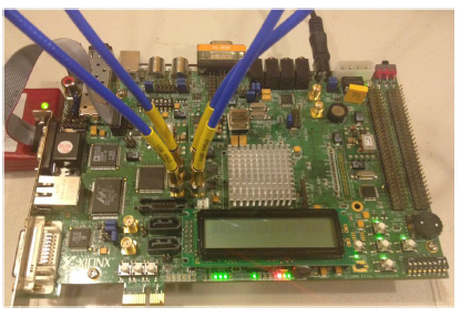
Fig. 1 Differential copper cables ASP1-024-ASP1-S402 form an external serial link, connecting transmitter and receiver pairs of GTP1 on dual tile GTP_X0Y5 integrated on the Virtex 5 FPGA on Xilinx XUPV5-LX110t board.
The RocketIO wrapper was created using the Xilinx ISE design tool CORE Generator®. The RocketIO offers useful features to support a wide variety of interface applications and transmission protocols. RocketIO has built in Physical Code Sub-layer features such as 8B/10B encoding, comma alignment and clock correction.
The comma detection and alignment circuit was activated to properly align 16-bit input data during the initialization of the data transmission process. Serial data must be aligned to symbol boundaries before it can be used as parallel data. To make alignment achievable, transmitters send a recognizable sequence, defined as a comma during device configuration. The receiver looks for that predefined comma in the incoming serial data. When it detects it, it shifts the comma to a byte boundary, so that the received parallel words match the transmitted ones. The GTP transceiver includes an alignment block that can be set to align specific commas, or to manually align data using bit-by-bit sliding.
The 8B/10B encoding includes special characters (K characters) that are often used for control functions. To transmit TXDATA as a K character instead of regular data, the TXCHARISK port must be driven high. If TXDATA is not a valid K character, the encoder activates an error signal. At the receiver end, RXCHARISK is asserted when RXDATA is an 8B/10B K character. This feature is not defined for bytes that bypass 8B/10B encoding. To mark the beginning of the valid data stream in the testing process, a K28.5 (10111100 = BC) character was sent. The K character was recognized by the receiver, and the RXCHARISK signal was set high. This control signal was used to trigger an address generator of the spike detection block, in order to assure correct address-data alignment. For transmission testing, the signals were monitored using ChipScope as shown in Fig 2.

Fig. 2 A screenshot of the ChipScope waveform window, showing transmitter and receiver 16-bit data split into lower and higher bytes (upper red signals). No data is available on the receiver end before it completes the reset operation and pulls ‘reset done’ high. TXCHARISK is a 2-bit input control signal at the transmitter end. TXCHARISK [1] corresponds to TXDATA [15:8] and TXCHARISK [2] corresponds to TXDATA [7:0]. TXCHARISK should only be asserted for TXDATA values defined by 8B/10B encoding as K-characters. At the receiver end, RXCHARISK is a 2-bit output signal that is asserted when RXDATA is an 8B/10B K character. Bit 0 corresponds to the lower byte of RXDATA, and bit 1 corresponds to the upper byte. The latency between sending the data at the transmitter data port, and receiving it as a parallel word was 18 clock cycles at a 125 MHz clock, and the target line rate was 2 Gbps.
Design Verification of the Spike-Based Data Reduction Unit:
The Spike-Based Data Reduction unit, handling 128 channels, was first simulated using Xilinx® ISim. After design simulation, it was implemented in hardware, and tested using ChipScope®. Modeling the data acquisition process, test neuronal data were saved on a BRAM, and then transmitted serially using MGT transceivers to the spike detection units.
The design verification objective was to make sure that the spikes have been detected and that their AP waveforms are copied to the output FIFO with the correct alignment required, correct time-stamp and channel ID.
For this test a window of 256 samples of neural signals recorded at 31.25KHz from, containing only one spike were stored on distributed ROMs and read in a cyclic mode. Using a multiplexer data was sent to selected channels in order to be able to perceive the correct channel IDs at the output buffers as shown in Fig. 3.
To save the spike waveforms on the ChipScope memory, a ‘READ’ signal was generated by the FIFO_RD_address_generator module, to indicate when spike waveforms were available for reading in the spike detection buffer. When complete spike waveforms were copied onto the output buffer of a spike detection unit, the upper-limit of the reading address of the buffer was updated. If the reading pointer was below the upper limit of the buffer, the “READ” signal was set high and the FIFO_RD_Address_generator incremented the reading address pointer. The ChipScope read the FIFO_data_out only when the ‘READ” signal was set high. At quiescent intervals, when the “READ” signal was low, the output data of the FIFO was not sampled for efficient use of the ChipScope memory.
Fig. 3. A screenshot from ChipScope® monitoring the data sent to the output buffer of the spike-detection based data reduction unit. The data width is 18bits. The two higher bits are prefix data, indicating whether the lower 16 bits represent: ‘00’ a spike waveform sample, ‘10’ a time stamp or ‘11’ a channel ID. The figure shows two spikes detected on channel 2048 and channel 2056. A spike was detected at time stamp 15. The inset shows the .coe file used to initialize the ROM on the FPGA that stored the neuronal data for this test. The spike waveform carries 46 samples: 10 pre-spike, 1 spike and 35 post-spike samples. The data was sent to ChipScope® BRAM when ‘READ’ signal was high.