In Testing Data Transmission using Real Data Recordings the PCIe data transmission was tested using real neuronal recordings from 2550 channels. The spike times were stored on BRAMs and a model was designed to mimic the Spike Detection Unit function. The design affiliated 48 words to every spike detected, and sent it via PCIe to the host PC. Testing the signal integrity and transmission operation on real neuronal data with typical bursting rates were the main objectives of the test. In this test, the main goal is to validate the design of integrating 20 spike-detection units and sending the spike detection waveforms using PCIe. The scheduling of data transmission between spikes detected across the 2560 channels, and the queue depths are monitored in this test.
The worst case scenario is having all channels recording synchronized spikes exactly at the same time stamp. Although this case was not witnessed in the real data recordings that were examined, this test serves to determine the capabilities of the system. The goal of the test was to test the functionality of the design as well as determine the maximum synchronous bursting rate that the system can handle before starting to skip spikes. The performance of the system is governed by the memory capacity and clock rates. It was also important to determine the queuing based delay in the described worst case scenario.
A block diagram of the complete test setting is shown in Fig. 1 The following sections present a description of each block.
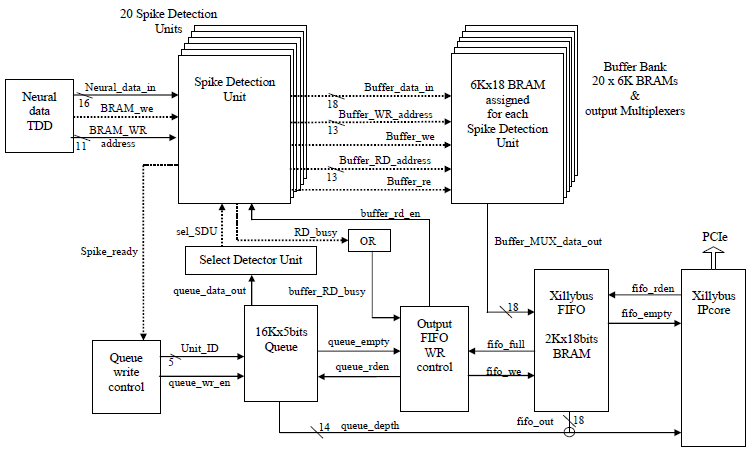
Fig. 1 Testing the integration of 20 Spike Detection Units (SDUs) on FPGA and using PCIe transmission to transfer detected spike waveforms to the host PC. The dotted arrows indicate that there are 20 replicates of similar internal signals each connected to one SDU. The solid arrows represent common or control signals.
Neural Data Time Division Demultiplexer:
The neural data TDD block has a ROM with stored neural data used for testing. It also has an address generator module that generates the time-stamp, the neural data ROM address, the channel ID, input BRAM_WR_address and BRAM_we. The virtual
sampling rate Fs, at which the channels are updated with neural data is equal to the address generator clock FTDD divided by the total number of channels Nch. The ROM has a short window of neural data containing only one spike that is being read
in a cyclic mode. Controlling the width of the data window determines the firing rate of the signal. A window of Nwindow samples having one spike and being read at cyclic mode at a rate FTDD has a firing rate FR of:

For example if:
FTDD = TDD clock = 50MHz
NCH = Total number of channels = 2550
Nwindow = Number of data samples read in cyclic = 256
The block has a data multiplexer to control the input data to each SDU. In this test, the multiplexer supplies the SDUs by either the data stored on the ROM or a zero signal. The total synchronous bursting rate was controlled by the number of channels supplied by the ROM data. The worst case scenario is modeled by supplying the same neural data to all channels handled in the system.
Queue Write Control:
The system has a queue FIFO that saves the temporal sequence of the detected spikes to schedule reading the spike waveforms from the output buffer bank accordingly. When a SDU completes saving a spike waveform on the buffer, it set a “spike_ready” signal high. The queue write control block uses a FSM to scan the SDUs for any completed spike signals. If a “spike_ready” signal is set high, it writes the corresponding Unit_ID in the queue to schedule a timeslot for copying the completed spike waveform from the buffer affiliated with that SDU. The “spike_ready” signal was added to the SDU design to serve the integration with multiple SDU and the data transmission to the host PC.
Spike Detection Unit:
The spike detection has three main operations in this test, namely:
(1) The spike detection using NEO operator
(2) Saving the spike waveform in the affiliated buffer
(3) Generating the Buffer_RD_address to send the data to the output Xillybus FIFO, when it is time to read from the SDU, following the queue schedule.
The first and second operation are managed by a SDU_FSM. In this design a “spike_ready” signal was added to mark the completion of copying a spike waveform onto the buffer. As this test involves a cyclic repetition of one spike, the autonomous threshold selection was not implemented and instead a fixed threshold was predetermined and used in the design.
The Buffer_RD_address generator features a pointer that saves the address of the last word read from its buffer. The SDU is selected to send a spike waveform to the output FIFO when its Unit_ID appears on the queue data output. When it is selected and the Output FIFO WR control activates the buffer_rd_en signal, the buffer_RD_address is gradually incremented until the 48 words of the spike waveform are copied to the FIFO.
While reading the spike waveform, the Buffer_RD_address generator sets a RD_busy signal high. This signal is connected to the Output FIFO WR Control module that manages the process of reading the spike locations from the queue. When the busy signal is activated by any of the SDUs, the queue_rden signal is set low.
The Queue:
The queue FIFO stores the ID of the SDU when it activates its “spike_ready” signal. The writing operation is managed by the “Queue Write Control” control module. The reading process is handled by the “Output FIFO WR control” block. The data output of the queue determines, which SDU is selected to transfer a spike waveform from its buffer to the output FIFO. The SDU keeps track of the last transmitted spike location on the buffer and hence this information does not need to be saved in the queue. The “Select Detector Unit” block activates the “sel_SDU” signal of the corresponding SDU defined by the queue data output.
The maximum queue depth was used to calculate the maximum transmission delay of the spikes to the Xillybus IPcore. The number of clock cycles that the system takes to copy a complete spike waveform to the Xillybus IPcore were determined using the ChipScope results. To monitor the queue depth, the data count on the FIFO was sent along with the spike waveform data via PCIe to the host.
The queue FIFO was created using Xilinx ISE core generator. The size of the queue was 16Kx5bits.
The Output FIFO WR Controller:
The output-FIFO-WR-controller manages copying the spike waveforms from the output buffer bank to the common output FIFO. It controls the reading process from the queue to decide which SDU should be enabled for a reading. If the queue is empty, or the system is busy reading a spike waveform from the buffer bank, or if the output FIFO is full, then the “queue_rden” signal is stays low. When the system is ready to read the next spike waveform, the “queue_rden” is activated for one clock cycle. Once the corresponding SDU is selected, the output-FIFO_WR-controller sets “buffer_rd_en” signal high to start the reading cycle of 48 spike waveform words. The output-FIFO-WR-controller manages the “output_FIFO_we” taking into account the reading and multiplexer delays between activating the buffer_rd_en signal and the data availability on the Buffer bank output.
The Buffer Bank:
The buffer bank has twenty 36K BRAM buffers, each assigned to one Spike Detection Unit. The outputs of the twenty buffers are connected via multiplexers to the buffer output. The “Buffer_MUX_data_out” is connected to the data input of the output buffer. The selection route of the multiplexers is determined by the Unit-ID that the queue outputs.
The Output FIFO:
The output FIFO has different reading and writing clocks. The writing clock is 100MHz supplied by the PCIe, and the writing clock is 50MHz. The slower clock was obtained by applying a counter supplied by the external 100MHz clock. The reading process from the output FIFO is controlled by the Xillybus IPcore as shown in Fig. 2.
Fig 2 A screen shot from ChipScope, describing the copying process of spike waveforms from the buffer bank of SDU_00 onto the output Xillybus FIFO, to the Xillybus IPcore and then to the PCIe link.
Test Results:
Monitoring the signals using ChipScope, it was observed that 58 internal clock cycles are needed to copy a complete spike waveform from the buffer bank into the output FIFO and get ready to read the next AP waveform. In other words the time between two successive queue read enable signals is equal to 58 clock cycles. Each buffer associated with a spike detection unit can hold up to 128 spike waveforms at a time, counting for the case when all channel s have detected spikes at the same time stamp. When a spike is detected a 48-word block of memory is reserved in the buffer, and the samples of the refractory period are copied to the buffer as they arrive to the input BRAM one by one. Hence in case of the perfect synchronous firing over all the channels, all the spikes need to be transmitted to the output FIFO before the next synchronized event occurs to prevent the dropping of any data. Assuming that the output FIFO will not be full at any of the transmission intervals, the maximum theoretical FR per channel that the system design can handle is:
The testing spike had 256 samples that were read in a cyclic mode, simulating a synchronous firing rate of ~76 spikes/sec per channel. The ChipScope screen shot in Fig.3 graphs the queue depth sent along with the spike data to the host. The figure shows that the queue is completely emptied before new spikes are detected on the Spike detection unit. The maximum delay, as shown in Fig.3 and Fig. 4, would be:
Fig. 3 In this test synchronous spike detection over all the channels was modeled, hence the queue depth is incrementing at every
internal clock cycle during the spike time stamp. The design module can read a new spike waveform every 58 clock cycles.
While a total number of 2560 channels are “reserving a turn” in the queue, the first 45 ( ~ 2560/58 + 1) spike waveforms are
copied to the output buffer. That is why the maximum queue depth is 2515 (2560-45).
Fig. 4 ChipScope bus plot of the 32-bit data words transmitted to the Xillybus IPcore. The higher 14 bits represent the queue depth while the lower 18 bits have a two bit header and 16 bits of either AP waveform data, a time stamp or channel ID.
Table 1 and table 2 present the device utilization and timing summary respectively:
Table 1 Device utilization summary for the hardware implementation of twenty spike detection units integrated with PCIe transmission.
Table 2 Timing summary of the same design setting.