After testing the data transmission from FPGA to the host, using continuous incrementing counter data, it was desirable to evaluate the data transmission and queue depths needed when the system is handling real neuronal firing rates on hardware.
As the spike detection platform is not connected to real data acquisition system, the data was saved on the FPGA block memories. With a limit of 148 BRAMs of 36Kbits capacity each on the Virtex 5 FPGA XUPV5lx110t, a reduced version of the main design has been tested. The test focused on the transmission key players, which involve the queuing-based transfer of 48 samples for each detected spike to an output FIFO connected to Xillybus IPcore. It also examined the queue depths needed to prevent any spike dropping before transmission, while considering the reading cycles on hardware. The block diagram of the test setting is shown in Fig. 1.
Simulations were run on neuronal data recordings using MATLAB. The spike detection results were reduced to the spike times and the corresponding channel ID. The data was presorted based on the spike times first then the channel order based on the Time Division Multiplexing. The created data file was used to initialize a ROM on the FPGA, which served as the source of spike timing in the transmission test. As a numerical figure, for 88928 spikes detected in a 2.5 sec recording time, there was a need for 73 BRAMs to save the results on FPGA. A Time Frame Generator was used to determine when the spikes are sent to the transmission queue.
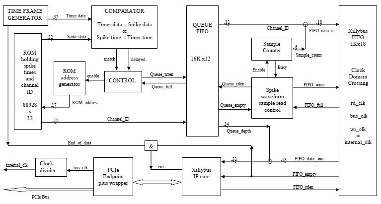
Fig. 1 A hardware design to test the data transmission of the detected spike wave shapes from the FPGA to the host PC based on spike timings obtained from real neuronal recordings.
When the time frame matches the saved spike timestamp and channel ID, the spike information is sent to the queue, and the ROM_address is incremented to read the next spike time. In case of synchronous firing, the timer may pass the next spike timestamp during the comparison and ROM reading cycles. If the time of the timer generator is greater than the spike time read on the ROM, the comparator activates a ‘delayed’ signal, and the controller sends the spike to the queue. The queue follows the temporal sequence of the detected spikes, and in the actual design, it holds the location of their waveforms in the output buffers of the spike detection units. In the reduced design used for testing, the 48 samples were generated using a sample counter, and they were concatenated with the channel_ID, and then sent to the output Xillybus FIFO. The FIFO input data is 18 bits long (12 bits for channel ID and 6 bits for sample order). The Xillybus IP core is designed to handle 32-bit words, so the 14 extra bits were used to send the queue-depth. The signals were monitored using ChipScope, and the data sent was evaluated using MATLAB.
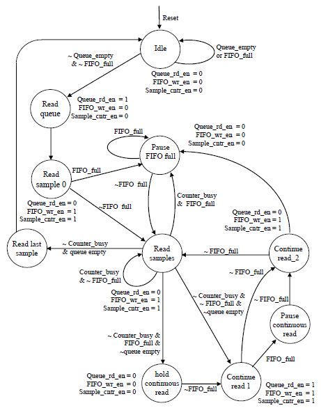
The testing design incorporates two controllers: One manages the timely flow of spike data from the ROM to the queue, as explained above, and the second controller manages sending the spikes read from the queue to the Xillybus FIFO after attaching 48 samples to each spike. The spike waveform sample read controller was designed using a FSM as shown in Fig 2. The sequence of sending the spike samples to the output FIFO starts by enabling the sample counter. The counter increments gradually, to represent the 48 spike wave-shape samples. When started it activates a busy signal that is set back to low after completing the count. The controller sets the counter to a pause mode if the FIFO is full. When the busy signal is deactivated, the controller generates a queue read enable signal if the queue is not empty. The Xillybus IP core handles the reading control.

Fig. 2 A description of the read sample controller FSM in the reduced design testing the transmission rate of spike waveforms via PCIe from the FPGA to a host PC.
Fig. 3 Design verification was tested using signal monitoring in ChipScope®. ChipScope was used to examine correct sample alignments, and validate read and write cycles. The integrated logic analyzer was clocked by the bus-clk running at 100MHz. Internal clock was 50MHz. The time between reading the spike from the queue to sending the waveform outside the Xillybus FIFO is 54 internal clock cycles = 1.08sec. No accumulation on the Xillybus FIFO.
Timing and Clocking:
Based on the timing summary generated by Xilinx® ISE Project Navigator, the maximum frequency, according to the critical path, is 65.811MHz. The 100 MHz clock provided by the PCI Express connector was connected directly to the Virtex-5 FPGA to clock the PCI Express Endpoint Block and PCI Express Endpoint Block Plus LogiCORE. The Xillybus IPcore and the reading clock of the Xillybus FIFO were supplied by the 100MHz clock denoted by bus_clk. Using a counter, an internal clock was generated, operating at 50MHz to regulate the rest of the design modules on the FPGA. The clock domain crossing was at the Xillybus FIFO, with the writing clock equal to 50MHz and the reading clock equal to 100MHz. In the complete design, if the TDM of for example 2500 channels, would be connected to the same internal clock of 50 MHz the design would allow a sampling frequency of 20 KHz per channel.
Device Utilization Summary:
The following is a table detailing the hardware usage to implement the transmission rate testing design. Table 1 utilization is based on the xupv5lx110t FPGA.
Table 1 Device utilization summary to implement the transmission rate testing design for real neuronal data firing rates.
Data Used in the Test:
The data used in the test were recorded from dissociated rat hippocampal cells (2 days in vitro) using high-density MEA from 3Brain (www.3Brain.com). They have been supplied by the NetS3 Lab in the Neuroscience department of the Instituto Italiano di Tecnologia (IIT). The sampling frequency was 7.022 samples per second. The recording duration was 2.5 seconds. Total number of spikes detected across 2550 channels during the 2.5 sec recording time was 88928 spikes. Hence the Mean Firing Rate (MFR) was:
Queue Depth Implementation Results:
The queue depth signal was sent along with the spike data for testing purposes as shown in Fig. 1. The instantaneous queue-depths were extracted from the data words received at the host and are presented in Fig. 4. The maximum TR of the spike samples to the output FIFO is determined by the reading clock of the Xillybus-FIFO. As the internal frequency was set at 50MHz, the Xillybus FIFO can read 50 MSamples/sec. With 48 data words per spike, the internal queue can be cleared at a rate of 1042,667 spikes per sec.
Applying the queue reading rate to the test data MFR and sampling frequency, the following can be concluded:
(1) The internal queue is read at a rate equal to 29.3 times the MFR.
(2) The time-stamp is based on the sampling frequency of the neural recording channels.
According to the testing design, no spikes can be detected between successive time stamps. With a sampling frequency of 7.022 KHz and a queue reading rate equal to 1042,667 spikes/sec, 148 spikes can be removed from the queue before any new spikes are added to it as shown in the inset in Fig.4 The maximum queue depth due to synchronized spikes was 184 spikes. Hence, the accumulation of spikes in the queue from one time-stamp to the next was limited to a few tens of spikes, if more than 148 spikes were detected at the same time-stamp. Removing 148 spikes from the queue means that 7104 words (148 spikes x 48 data-words/ spike ) were read by the output FIFO. The difference between the two instances marked by the data-tips in the inset of Fig. 4 validates this statement.
The maximum queue depth in hardware implementation was 184 spikes as shown in Fig 4, while the maximum queue depth in the MATLAB model was 780 spikes. This difference was caused by the binning of spikes into 1msec intervals in the MATLAB model. The binning accumulated the spikes read across seven sampling periods (1msec bin/sampling period). The bin size choice of 1msec was relatively large with respect to the MFR of a few thousands of bursting neurons. A bin size equal to the sampling period (conforming to the time-stamp rate) is expected to match the hardware implementation results. Fig.4 is more dense than Fig.5 because of the fact that the quiescent intervals with clear empty queue were not monitored by the host as the PCIe transmission was idle during these times.
The MATLAB model, with a 1ms bin size, was run on a PC featuring an AMD Phenom™ II X6 1090T Processor 3.20GHz and a 64-bit operating system. The calculations of the queue-depth took approximately 12 hours to complete. The hardware implementation was much faster, taking less than a second.
Fig. 4 The figure displays the queue depths after being extracted from the data sent via PCIe. For a total of 88,928 spikes, 4,268,544
(88,928 x 48) data words have been received. The inset shows how the design module clears 148 spikes from the queue
between successive synchronized firing time-stamps. The recording sampling frequency was 7.022KHz.
Fig. 5 The figure displays the queue depths after being extracted from the data sent via PCIe. For a total of 88,928 spikes, 4,268,544
(88,928 x 48) data words have been received. The inset shows how the design module clears 148 spikes from the queue
between successive synchronized firing time-stamps. The recording sampling frequency was 7.022KHz.