System Overview:
The Neural Spike Detection platform receives time division multiplexed serial samples from a high number of neural recording channels at the multi gigabit receiver port of the FPGA. The receiver performs deserialization of the data and ensures correct sample-word alignment. The system affiliates each sample to its source channel and performs spike detection. If a spike is detected the spike waveform along with its time stamp and channel ID are passed to an output buffer for further spike sorting or data analysis. Fig. 1 presents the integration of the spike detection platform in a typical neural signal processing system.
The typical neural signal processing pathway starts with a data acquisition system that records extracellular potentials from an MEA. The data acquisition provides amplification, filtering, time division multiplexing and A/D conversion of data read from the different electrodes. Then the signal passes through spike detection followed by spike sorting, spike binning and analysis. The dissertation work focuses on the spike-based data reduction module and is thus concerned with the interface between the ADC of the data acquisition system and the interface with the spike sorting on FPGA or sending the data to a host PC for further analysis.
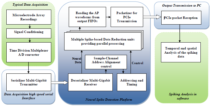
Fig 1: A block diagram of the Neural Spike Detection platform and its integration in a Neural Signal Processing system. The center block (dark blue) presents the Neural Spike Detection (NSD) platform performing spike-based data reduction. The blocks (light blue) connected to the NSD platform on the left and right sides present the interface required to embed the platform into a NSP system. The upper left and bottom right (green) building blocks present typical neural data acquisition and spiking analysis on a host PC, respectively. These are not part of the dissertation work.
The detection platform performs spike-based data reduction where:

where MFR = Mean Firing Rate. For example, for a MFR of 18 spikes/s/electrode, 50 samples per AP waveform, and a sampling frequency of 40 KHz the reduction ratio = 0.025.
As the system is designed to handle thousands of recording channels, it has to offer enough bandwidth to receive the massive amount of neural data from the data acquisition system in real time. For example for a 2560 channels sampled at 31.25 KSps, and a precision of 16-bits per sample, the data rate has to be 1.28 Gbps. Consequently, the platform architecture integrates the application of high-speed serial transceivers to allow for the required input data transmissions.
Although, the amount of data is significantly reduced, the system needs to integrate a high-speed communication link to transfer the AP waveforms to the host PC, accounting for transmission bottlenecks during periods of multi-channel neuron bursting. A PCI express link is integrated to minimize queuing-based transmission latencies and performance degradation when the output data overwhelms the transmission
bandwidth of the device.
Spike-based Data Reduction Unit:
The main building block of the design architecture is a spike-based data reduction unit that handles 128 channels. This unit can be replicated to process a higher number of recording sites. A block diagram of the spike detection module is shown in Fig.2 The spike detection unit receives time division multiplexed 16-bit sample data from 128 channels; it tests the samples for possible spikes, and then sends the complete Action Potential (AP) waveform of a detected spike preceded by the time stamp and the channel ID to the output buffer memory. This section presents the main building blocks of the unit and indicates how the design parameters were selected based on the spike detection algorithm applied on the platform. The main building blocks of the spike detection units are:
- 3.2.1 The Spike Detector
- 3.2.2 The output Buffer
- 3.2.3 The Input BRAM
- 3.2.4 The Channel Status Module
- 3.2.5 The BRAM Read Control
- 3.2.6 The Operation Management FSM
- 3.2.7 The Autonomous Threshold Selection
Fig 2: A block diagram describing the spike detection process. The spike detection unit is designed to detect neural spikes over 128 neural signal recording channels.
The Spike Detector:
The Spike detector block holds the hardware implementation of the spike detection algorithm. Various spike detection algorithms with different levels of complexity and performance have been presented in literature and can be applied on the designed
platform with proper modifications of the system design parameters. As an example, the design model applies spike detection based on the absolute threshold after passing the signal through a Nonlinear Energy Operator (NEO) preprocessor eq.3.2 in order to give emphasis to the spikes relative to the noise and consequently, improve the spike detection performance.
where x[n] is the neural data sample at any instance n.
The threshold for a given channel is set to a multiple of an estimate of the noise level on that channel.
The Output Buffer
A neural AP has duration of ~ 1.5ms on average. Considering sampling rates in the range of 30 KHz and based on the wave-shape, a full AP waveform was assumed to have 10 prespike samples, 1 spike sample and 35 samples representing the spike refractory period. This assumption was optimum for organizing the FIFO memory and address assignment. The output FIFO memory 3x36K can hold up to 128 spike waveforms at a time, counting for the worst case scenario if firing neurons are detected on all channels at the same time. When the unit receives a sample from one of the channels it is written in the input memory.
Fig. 3 (a) Spike counter and Base address look-up ROM used to determine the first available memory space in the output buffer to store a detected spike AP.
(b) Organization of the output buffer.
The Input BRAM:
For spike detection consecutive samples are needed to identify a spike. Each channel is assigned a memory space on the input BRAM to hold the most recent 16 samples. The depth of the memory space assigned to each channel was chosen to hold enough sample history to acquire the ten pre-spike samples, the spike sample x[n] and five post-spike samples. Four of the post-spike samples are the “future” samples held to reach x[n+4] needed for the NEO computation, and x[n+5] is added for timing control, as would be explained in the operation management section. The design does not copy the AP waveform as a bulk to the output buffer, instead it copies the first 16 samples, and then sends the refractory period sample by sample as they arrive at the input BRAM. This scheme has minimized the memory space depth needed for each channel, saving on total memory usage. An example of the arrangement of samples in the input BRAM space assigned to one channel is shown in Fig. 4
Channel Status:
Switching between multiple time multiplexed channels with different statuses requires holding the status of each channel to determine the operation to be applied on the respective incoming input sample. The channel_status memory holds 128 words describing the status of each channel handled by the spike detection unit. Each word has fifteen bits. Two bits describe the state of the channel, and 13 bits hold the FIFO address needed to copy the AP samples at the right location and space assigned for it on the output buffer in case a spike was detected. The channel status bits and the cases they represent are shown in Table 1.
Fig 4 An example of the arrangement of samples in the input BRAM space assigned to a channel k, when a spike is detected and when the initial part of corresponding AP waveform is copied to the output buffer.
Table 1: Channel-status-bits and the corresponding status description
The BRAM Read Control:
When the unit receives a sample from one of the channels it is written in the input memory. The BRAM read control checks the status of the channel being updated and plans the reading procedure accordingly. The channel_status word can indicate 3 possible cases:
The BRAM Read Control:
In this case the incoming sample is sent to the NEO module and threshold comparator for testing. If a spike is detected, a memory block space of 48 words is saved in the buffer to hold the corresponding AP waveform. The spike detector unit has a spike counter that is used along with a look up ROM to determine the first output buffer memory space available for AP waveform storage as shown in Fig. 3. If a spike is detected, the counter is incremented, and the time stamp and channel ID of the detected spike are copied into the lower first available buffer address indicated by the look up ROM. The channel_status word is updated to save the block base address that saves a space on the output buffer to hold the AP waveform. This case is represented by a channel-status = 00.
(2) The channel has a detected spike and a saved memory space in the buffer:
In this case the reading control copies the first 16 samples of the AP waveform available in the input BRAM to the output buffer memory. (10 pre-spike samples, 1 spike sample, 4 post-spike samples required for the NEO and the incoming sample) This is the longest cycle of the copying process. It takes a total of 19 clock cycles to complete. The unit has to complete it before reading a new sample. This case is described by a channel-status = 01.
(3) The refractory period of the AP waveform is being completed:
The incoming sample is copied directly to the output buffer. The 35 samples of the refractory period are each copied upon arrival at the input BRAM to the output buffer. This step is repeated 35 times to complete the refractory period. At each cycle the channel_status is updated with the buffer address that will hold the next incoming sample in the refractory period. Once a spike waveform is completely copied to the output buffer, the BRAM reading control updates the upper-limit for the buffer emptying process. The two states (10 and 11) were split into two states to apply an address counter for the lower 4 bits of the buffer address only, instead of applying an address counter for the whole 13 address bits. The 9 most significant address bits are updated the when the channel moves from state 10 to state 11.
The AP refractory period arrives in single samples at the output buffer. Once the last sample arrives at the input BRAM, it is directly transmitted to the output buffer and the complete waveform becomes available for further processing or transmission to a host PC. The design avoids queuing-based transmission, that arise from copying the AP waveforms as a whole to the output buffer. The memory space assigned for each channel on the input buffer memory is also reduced. The spike detection module and output buffer have access to read data samples from input BRAM.
Operation Management:
To control the sequence and timing of operations, a controller employing a finite state machine is used. Figure 4 presents an overview of the BRAM read control state diagram. The channel status word has two bits describing the spike copying stage. They are used to decide whether input stream should be passed through the NEO detection module or copied directly to the output FIFO.
Figure 5: Overview of the state diagram describing the controller operation
Autonomous Threshold selection:
With the high channel count automatic threshold selection for each channel is vital. After reset, the system starts computing the threshold for each channel as a multiple of the Mean Deviation MD of a window of its incoming data. The channels are disabled until their thresholds are calculated, and saved on a threshold RAM. Fig.6 describes the details of the NEO preprocessing, threshold comparator operation and threshold computation.
In the normal operation, the samples are passed through the NEO module, the computed output is compared to the threshold of the corresponding channel. In the case of threshold computation, the output of the NEO is passed to a MD computation,
where N is the window size of the data being used to measure the background noise. N is chosen to be a power of 2, so that the division by N can be performed by rightshifting of the dividend. Based on the threshold selection guidance provided in literature the multiplier is chosen to be 16.
Each channel is affiliated with two bits in the enable-disable queue register that determine the state of the threshold computation. The enable disable queue is used to determine whether the channel is disabled (11) as it still does not have a computed threshold yet, or whether the channel is undergoing a threshold computation (10), or if the channel has a valid threshold and is enabled for spike detection (00). The register is shifted 2 bits to the left whenever one channel has finished the threshold selection.
Fig.6: Block diagram describing the NEO preprocessing, threshold comparator and threshold computation