Introduction
In the literature, the existing tactile imaging sensor system (TIS G1) has proven to be successful in capturing tactile images and measuring mechanical properties (Lee and Won, 2011). However, the dimensions of PDMS in TIS are 2.3cm × 2.0cm × 1.2cm, which limits the size of the detection area of TIS G1. In addition, the images provided by the TIS G1 are blurring images of a target because the camera in TIS G1 focuses far away from the contact surface of this device. In TIS G2, we want to obtain clearer images of the PDMS probe and target interactions. Also, LED illuminating circuit is a simple resistor circuit, where the light intensity is not stable and hard to control. Thus, our goal for this section is to design a second generation tactile imaging system (TIS G2) to detect larger area, provide stable light brightness and obtain the clear image of the target. In other words, we should distinguish the shape information for different targets. To make TIS G2 more portable, we will also design a possible upgrade for the external force sensor.
Requirement and Challenge
TIS G1 detects target through the touch sensation, which is similar to the way physicians use palpation to detect breast tumors. Physicians use fingers to feel unhealthy tissues which tend to be stiffer than the healthy tissues (Fung, 1993) (Krouskop et al., 1998). Average pad of the human finger is 10 to 14 mm wide and the average fingertip is 8 to 10mm wide (Wroblewski, 2010). We would like to make the contact area as big as the palm of hand; however, there are some difficulties to have such a large contact area. First, we need more LEDs to emit light and that needs more battery to support the LED circuit which will increase the size and weight of ours device. Second, it’s hard to keep the light even within the waveguide. At least, the bigger the waveguide, the easier the light is disturbed by outside interferences. Thus, we will first design the configuration of the light source for the probe.
We plan to obtain clearer shape information. For the first generation TIS, when we detect targets which have different shapes, we get round images for all the targets. That is because the focus point of lens is far away from the surface of the probe. A lens can precisely focus objects at a distance; objects at other distances are defocused. On the other hand, we want to make TIS G2 as small as possible, which restrict our choices of the lenses with short focal distance. In order to get clearer image and minimum size of the device, we need to make our camera focal distance small.
The third challenge is to build a constant current driver circuit small enough to be attached on the side of the camera. There are a lot of constant current driver modules available in the market. However, if we use them in our design, we will need a high voltage source to drive all the LEDs. In that way, we need a large space for the battery. But in our project, we want to arrange all the parts around the camera, so the space is limited. Therefore, we need to design a circuit as small as possible with a lower voltage input requirement.
When we calculate the mechanical properties of the targets, we need to utilize the compression information, which correlates which each image. Thus, in the experiment for both TIS G1 and TIS G2, we have to connect a force gauge on the top of our device to obtain the force information. In our clinical practice, not all the doctors are comfortable with this method. Thus, at the end, we will introduce a possible upgrade for force gauge part.
Hardware Design
In this design, since we are focusing on the hardware improvement, and in order to minimize the software modification, we keep using the TIS G1’s camera and computer interface in TIS G2. 12
The TIS G2 will also incorporate a light source unit with PDMS optical waveguide, a camera unit with lens and tubes, and a computer unit to analyze the data. The camera in TIS G2 is the same CCD camera F044B-NIR and connected to computer using IEEE 1394A firewire. Following section will introduce the hardware modifications.
Lighting Source Configuration
First, we design the lighting source of TIS G2. A large PDMS would make it harder for the LED light to distribute evenly inside the PDMS. In this design, we use 3.8cm × 3.8cm × 1.4cm PDMS, which has a similar size of four fingers. In TIS G1, simple single LED are arranged on four sides of PDMS to provide the light. We first tried this method. We used the same 1500 mcd LEDs and put them in the middle of each side as shown in Fig 1 However, just four LEDs are no longer sufficient to light up the whole area of PDMS. So we also tried higher intensity 3000 mcd LED, the tactile image for a 15 mm white ball is shown in Fig 1 Instead of showing the round image, the lights from four sides are stronger than other areas, which change the shape of the target. We also tried using the flat top wide angle LEDs, which have 105˚ -120˚ viewing angle. However the image did not get much better.
Figure 1: The Schematic of Initial Design of TIS G2 and the Image
After these tests, we decide to use 8 LEDs to light up the PDMS, and each LED has rating of typical forward voltage of 3.6 V, a forward current of 20 mA and a viewing angle of 25°. We changed the circuit to drive 8 LEDs, and constructed two designs. For the first one, we put two flat top LEDs on each side of PDMS, and for the second one, we used a nylon tube as the diffusing lighting tube and put two regular LEDs on the two sides of nylon tube. These two designs are shown in Fig 2. After comparing the images of these two designs, the second one give us better image of the target, but the camera also captures some light from the LEDs from four corners, which results in distortion of the image. To avoid that light, we decided to use black tape cover the margins of nylon tube.

Figure 2: The Schematic of Second Design of Lighting Part
Lens Selection
To get a clear image for the target, we need to choose another lens to focus on the surface of PDMS; in the meanwhile we want to keep TIS G2 as small as possible in size. Therefore, the lens should have small minimal focal distance and large picture size at minimal focal distance. Our camera is AVT Guppy F044B, which has C-Mount lens interface. We searched different wide angle C-Mount lenses. After comparison, the Kowa LM6JC lens has smallest minimal focal distance (less than 0.1m) and largest shooting range, which is the best option for our design.
Table 1: A List of Data for Different Wide Angles Lens
Constant Current Driver Circuit
In our design, the probes are lit up using 4 semitransparent nylon tubes and each nylon tube has two ultra-bright white LEDs on both sides. The intensity of each lighting tube affects the pixel values of the captured images. The pixel values are very important, since we use these values to calculate depth, size and elasticity of the embedded targets. Therefore, having an uniform amount of light in each lighting tube and throughout the entire probe is an essential condition.
In the LED illumination circuit of TIS G1, four 1.5 V battery is used as a voltage source and the four LEDs are connected in parallel. Therefore, the voltage across each LED is the same. However, LEDs manufactured in different batches may have difference resistance, so the light intensity, may be different. Figure 4 shows comparison results among random six LEDs. Even for the products from the same batch, the forward current at given voltage varies widely. From Figure 3, we can find out that the current is approximately exponential function of voltage, which means a small voltage change may result in a large change in current (Maxim Integrated Products, Inc, 2004). Thus, it is not a reliable solution to drive LEDs using a constant voltage.
Figure 3: Forward Current versus Forward Voltage for Six Random White LEDs (three from each of the two leading manufacturers) (Maxim Integrated Products, Inc, 2004)
In order to ensure all LEDs are provided with same amount of current, all LEDs should be connected in series. In addition, a constant current driver should be used to stabilize the light output over a range of input voltage, which can increase the life of batteries. Having constant current driver can also help to avoid violating the absolute maximum current rating and reliability. Moreover we can obtain predictable and matched luminous intensity and chromaticity from each LED by driving all LEDs with constant current.
There are many different kinds of constant current driver having a wide range of price and function. In most of LED circuit designs, an integrated constant current driver module is used to drive the LED circuit, like step-down constant current source. However, the dimension of this module is 22.10 mm × 12.55mm × 8.50mm, which is not small enough for our design. In our design, we plan to attach all the parts around the camera, so we want to build our circuit as small as possible. The other reason the step-down series is not suitable for our design is that we need large space to arrange the batteries. Since in a step down source, the input voltage need to be greater than the LED’s operating voltage, which is 28.8 volt (3.6volt × 8 LEDs). In this case, we need at least ten 3V batteries or four 9 V batteries. Another idea is to add a boost up circuit to reduce the number of batteries. However, the extra circuit may add complexity to our design. Therefore, the integrated constant current driver module is not a good option for our design. Therefore, we decide to build a circuit by using small IC chips and other circuit components.
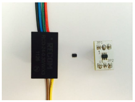
For the constant current driver chip, what we need is a small size chip, which can drive at least 8 LEDs in series using the smallest possible amount of input voltage. After researching some boost up driver chips, we find out the LT1932 constant current DC/DC LED Driver of ThinSOT Chip is the best option. It has wide voltage range of 1V to 10V and can drive eight LEDs in series connection from 3V. In this case, we can drive the circuit using only one battery. The current through each LED can be fixed between 5mA and 40mA using different value external resister. It also provide the dimming control function to adjust light using either a DC voltage or a pulse width modulated (PWM) signal. Using this chip, we do not need extra boost up circuit, a signal battery greater than or equal to 3 V will solve the power problem. Moreover, we control the light intensity by add dimming control circuit. However, the chip is packaged in 6-lead plastic SOT-23 package and the dimension is about 3mm × 1.75mm × 1mm, which is too small to solder on the PCB board. Thus we need a SOT-23 to DIP adapter (10.16mm × 7.62 mm) to connect it into the circuit. Fig. 9 shows the comparison among the RCD series driver module, LT1932 and L T1932 with adapter.
Figure 4: The Pictures of RCD Series Driver, LT1932 Chip and LT1932 Soldering on the Adapter
In the datasheet of LT1932, there is an example circuit, which can drive 8 LED using wide range voltage from 3volt to 4.2 volt. It also provides the part numbers of the best fit components. However, all the suggested components are SMD (surface-mount device) component. Since it is very hard to solder SMD component on the PBC board, we decide to find DIP (Double In-line Package) replacement according to the component selection requirement. Figure 6 is the example circuit using LT1932 to drive 8 LEDs.
Figure 5: Example Circuit of LT1932 to Drive 8 LEDs
After comparing different types of battery, the lithium battery was chosen as the best option in order to provide a maximum amount of operating hours. The Tadiran 3.6V coin cell lithium offers a capacity of 1.7Ah, which provide much more operating hours than other types of batteries. In addition, the small dimension (ø 32.9mm × 10.2mm) allows us to attach it to the side of a camera.
According to the application information in the datasheet, for the inductor selection, since the core losses at 1.2MHz, which is much lower for the ferrite core, the ferrite core is a better option than the cheaper powdered-iron ones to obtain higher efficiency (Linear Technology Corporation, 2001). This design requires the inductor to handle at least 0.5A have a low DCR (copper wire resistance) to minimize I2R power losses and give two optional inductor value, 4.7μH and 6.8μH to satisfy the overall system efficiency. In our design, we chose 78F4R7J-RC (BOURNS JW MILLER), which has 38 MHz self-resonant frequency, 530mA direct current (DC) current rating and 0.35 Ω DC maximum resistance.
For capacitor selection, in order to decrease the output ripple voltage, a low ESR (equivalent series resistance) capacitor should be added at the output side. Multilayer ceramic capacitor should be an excellent choice for the output capacitor. A 1μF or 2.2μF output capacitor in X5R or X7R type is preferred. Thus, we used 1μF-50V-X7R capacitor 2C20X7R105K050B (VISHAY SPRAGUE) in our circuit. For the input decoupling capacitor, we also used a ceramic capacitor. We placed it on the left side of the LT1932 and as close as possible to it. The datasheet also offer us two value options, 2.2μF and 4.7μF. We used 4.7μF-50V-Z5U capacitor C340C475M5U5TA (KEMET) as the input capacitor.
For diode selection, the datasheet suggest us to use Schottky diode, because it has low forward voltage drop and fast switching speed. Furthermore the voltage rating of this diode must be greater than the output voltage. A 1A-40V-SOD323 Schottky rectifier ZHCS400 (DIODES INC) was used in our circuit, and the diode just conduct current when the power switch is turned off.
For the resistor, a single setting resistor is used to set the current for each LED. This resister is connected to the RSET pin, which is internally regulated to 100mV. The current flows out from the pin ISET, and the value is calculated using 100mV/RSET . The current goes into the LED pin,ISET , is 225 times of the value of . Thus, for different LED current values, the RSET can be calculated using the following equation,
In our design, we want the white LEDs to be driven at maximum currents of 20mA, so the value of RSET will be 1.13kΩ.
For the chip LT1932, there are two ways to control the light brightness. First one is to use a variable DC voltage to adjust the LED current and the other one is using PWM signal. In our design, we just use batteries to power the circuit, and we want to get as much life time from the batteries. We decided to use PWM dimming control, because this method is more energy efficient. The PWM brightness control function pulses the LEDs on and off using the control signal and the average current changes with the PWM signal duty cycle. Typically, a 5 kHz to 40 kHz PWM signal is used for LT1932 applications (Linear Technology Corporation, 2001). In our design, we accomplish PWM dimming use pin with a resistor. In this way, the LEDs will be decreased the brightness by increasing the duty cycle and turned off completely using SHDN. The approximate value of should be calculated using following equation, where the is the high pulse value of the PWM signal.
To obtain a PWM signal, the most common method is to generate it from a microcontroller, but we need to program the microcontroller, which is not the easiest method for our design. The other common method is to use LM555 Timer to build a PWM generator. However, the minimum supply voltage for LM555 chip is 4.5 V, which is greater than our 3.6 V power supply. After researching different designs for PWM generator, a PWM circuit designed by David Cook has wide input voltage range from 2 V to 6 V. We decided to use this design. Figure 7 shows the original design by David Cook. We needed to modulate some components to get our required PWM signal.
Figure 6: The PWM Circuit Design (Cook, 2007)
A PWM signal is a rectangular voltage pulse wave signal which generated by making the voltage goes up and down repeatedly. The circuit in above figure uses RC timing with a diode twist to change the duty cycle, which is the ratio of the on-pulse time versus the off-pulse time (Cook, 2007). This IC chip is a 74AC14. This chip is designed with Schmitt-trigger inputs which can efficiently convert slowly changing or analog signals.74xx14 is the standard number of hex inverter and AC means advanced complementary metal oxide semiconductor (CMOS), which indicated the chip has wide input range from 2 V to 6 V and the output current is up to 25 mA. The chip 74HC14 and 74LV14 also can generate PWM signal, however the voltage range or output strength cannot match the 74AC14. In this design we just use two inverters. It’s better to have small dual inverter in our design, but we did not find any dual inverter chip which has Schmitt-trigger input and the same wide input range, so we just use this six inverter chip.
For the compounds in this circuit, C1 is the input capacitor to smooth the power supplied to the chip and avoid intermittent glitches on the inputs or spikes on the outputs. The author Dived Cook used 0.1 μF capacitor in his design, so we keep use this value. C2 is the capacitor to be filled up and drained repeatedly to make the pulse wave and the value of this capacitor will affect the frequency of the signal. Increasing the capacitance decrease the frequency of the wave and decreasing the capacitance increase the frequency of the wave. R2 is a variable resistor to change the duty cycle of the output wave and the value of the total resistance value also can change the frequency of the wave. In our design we chose 0.01 μF capacitor and 10 kΩ potentiometer to generate a 10 kHz PWM signal. For the two diodes D1 and D2, one is the charge path, and the other is discharge path. We used 1N914 diode in our design.
Figure 7: Schematic of Constant Current Driving Circuit with PWM Dimming Control